kuniga.me > NP-Incompleteness > Von Neumann Architecture
Von Neumann Architecture
10 Jun 2019
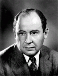
John von Neumann was a Hungarian-American mathematician, physicist, computer scientist and polymath, often regarded as the greatest mathematician of his time. He has contributed to a wide range of fields including quantum mechanics, geometry, topology, game theory, cellular automata, linear programming and computer architecture.
In this post we’ll discuss his contribution to the architecture of modern computers, known as von Neumann architecture (aka Princeton architecture).
Historical Background
Von Neumann was working at the Manhattan project, which required a lot of computation (in particular to solve differential equations). He got involved on the design of the EDVAC computer together with J. Presper Eckert and John Mauchly and together they wrote a document titled First Draft of a Report on the EDVAC [1]. For an unfortunate reason the report circulated only with von Neumann’s name on it, and the architecture based on the report has only von Neumann’s name [2].
Furthermore, around the same time Alan Turing, who proposed the concept of stored-programs in the form of theoretical Universal Turing Machines (in the paper On Computable Numbers, with an Application to the Entscheidungsproblem), also wrote a paper Proposed Electronic Calculator, discussing the practical aspects of constructing such machines.
These independent approaches led to a debate on whether stored-program machines should really be referred to von Neumann machines.
Overview
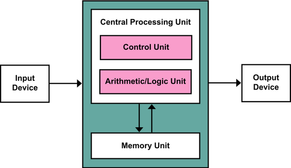
The architecture consists of 5 specific parts [1]:
(i) Central Arithmetic (CA): an arithmetic logic unit (circuit capable of performing elementary arithmetic and bitwise operations) and a set of registers (small fast-access memory).
(ii) Central Control (CC): a general purpose unit to carry out the execution of the instructions, to be stored elsewhere.
(iii) Memory (M): to store data during the program’s execution and also to store the program’s instructions. The draft also specifies that there must be a way to connect between these 3 parts. It’s interesting the analogy it makes to the human brain:
The three specific parts CA, CC (together C) and M correspond to the associative neurons in the human nervous system. It remains to discuss the equivalents of the sensory or afferent and the motor or efferent neurons. The external world is represented by the external medium, called R (which is not considered a part of the machine).
(iv) Input mechanism (I): a way to transfer information from R to C (CA + CC) and M.
(v) Output mechanism (O): a way to transfer information from C and M to R. The authors in [1] also pose an interesting question on whether information should be stored in M or R. Supposedly R representing some sort of external memory. It does resemble a more modern debate on volatile (RAM) or persistent memory (disk).
Modifications
One bottleneck of the original von Neumann machines is that both data and instruction go through the same bus. This is a potential limit on speed because data and instructions cannot be read in parallel.
The Harvard architecture doesn’t have this issue by separating out the memory (or at least having dedicated channels of communication with the central unit) and was implemented in the Harvard Mark I computer [3].
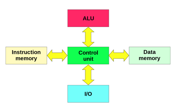
However, there might be advantages of treating both data and instructions as data since this allows for concepts such as just-in-time compilation where instructions might be written to memory during runtime and read as data. Modern computers (ARM, x86) use the so-called Modified Harvard architecture [4] which overcomes the bottleneck from von Neumann architecture by having a dedicated memory with a copy of the program (in the form CPU cache) but instructions can still be read as data when needed.
Limitations of classical architectures
We’ll now focus on the limitations of current implementations of the Modified Harvard architecture. It’s really hard to make any concrete estimates on the limitations of the early architecture proposals because they’re very high-level and the actual implementation might vary widely.
Processing Power
In 1965 Gordon Moore, founder of Fairchild Semiconductor, wrote a paper predicting that the number of transistors in the CPU would double every year for the next decade. The industry was eager to follow this prophecy and the trend followed for several decades (it was later adjusted to every 2 years), but it slowed down in the early 2010s. As of today, CPUs have in the order of 10’s billions transistors.
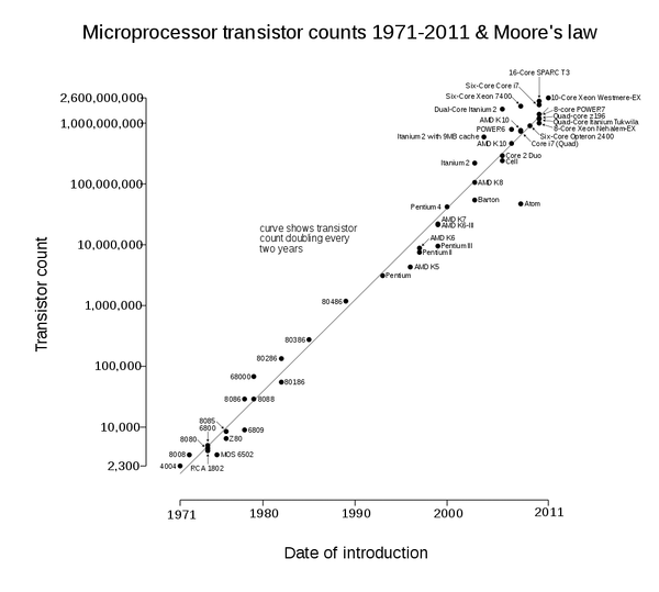
It’s impractical to think that we’ll be able to put more transistors in a chip forever since there are physical constraints. The question is what kind of constraints are we going to hit?
To pack more transistors in a chip we have to increase the size of the chip.
Increase the size of the chip. this incurs in more power consumption and heat dissipation and information has to travel longer distances, making computation potentially slower. Furthermore, large chips might be infeasible for small devices like smartphones.
Reduce the size of the transistor. For the current transistor design the size has a hard lower bound of the Silicon atom, which is about 0.2nm [6], but before we get there, we have to figure out how to manufacture them with such precision in a cost effective way. As of today, 14nm seems to be the smallest size that can be viably produced.
One question we need to ask ourselves is how having a large number of transistor in a chip translates into computing power? It’s a convenient proxy for CPU performance because it’s easy to measure. However, what can we achieve with more transistors? It allows higher parallelism via multiple cores and transistors can be used to build CPU caches, which improves the speed of common operations.
Other ways to potentially increase processing power is to keep the number of transistors constant but reduce the chip size. This decreases the distance needed for electrons to travel and by dissipating less heat, it’s possible to increase the clock frequency.
Besides reducing the size of the transistor, other strategies are being explored to reduce the chip’s area: instead of the classic 2D square layout, chip manufacturers are exploring stacking approaches to reduce the overall size of the chip.
Memory Bandwidth
The speed improvements of RAM memories haven’t followed the ones from the CPU. The widening gap can become so large that memory speed will become a bottleneck for the CPU speed (known as the Memory Wall [8]).
To work around this limitation CPU cache is currently being used. Alternative solutions include adding an in-chip memory to reduce latency in the transportation of data.
Related Posts
Mentioned by Function Objects in C++.
Conclusion
I didn’t have a good idea of what to write, but I was interested in understanding how close we are to practical limits of current computer architectures, so the idea was to go back to the early inception of computer architectures and learn some about it.
We’ve made rapid progress in the early days and had steady progress for a long time, so it’s reasonable to be optimistic, but progress has been slowing down, at least in the general purpose single-node computation. We’ve seen specialized hardware take place with GPUs and TPUs, and also the increase of parallel, concurrent and distributed computing.
Quantum computer still seems a dream far away. I wonder if there’s any value in rethinking the classical architecture model from scratch to see if we can escape from local minimum?
References
- [1] Introduction to “The First Draft Report on the EDVAC”
- [2] Wikipedia - Von Neumann architecture
- [3] Wikipedia - Harvard architecture
- [4] Wikipedia - Modified Harvard architecture
- [5] Wikipedia - Transistor count
- [6] Is 14nm the end of the road for silicon chips?
- [7] Intel demos first Lakefield chip design using its 3D stacking architecture
- [8] Wikipedia -Random-access memory: memory wall
